
Chinese tech firm launches GPU chip it claims marks ‘new era’ for computing
- Biren Technology says the peak performance of its 7-nanometre chip – made by TSMC – is three times better than equivalent products on the market
- It will be used in large-scale, cloud-based AI training in data centres and the company aims to partner with firms such as server provider Inspur
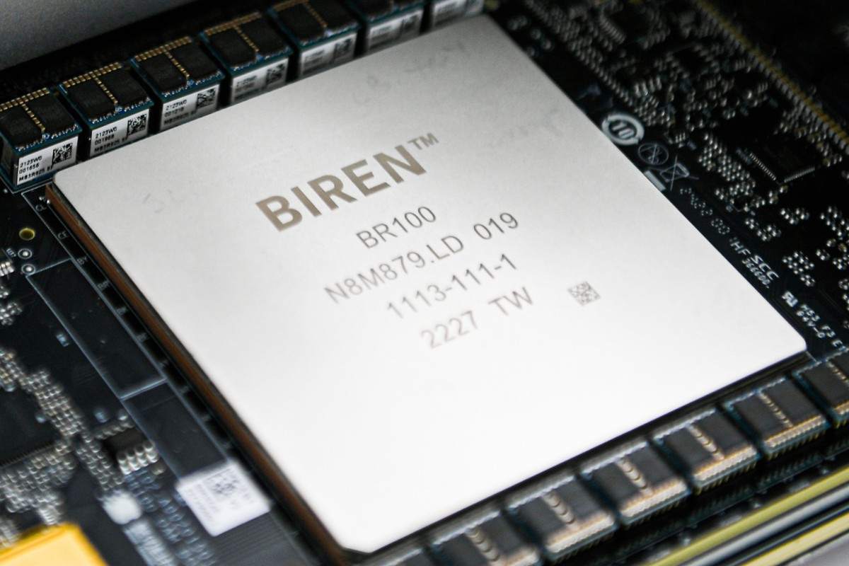
Biren Technology said in a statement that the peak performance of its BR100 chip, which was launched on Tuesday, was three times better than equivalent products on the market.
“This marks a new era, with China’s GPU chips being capable of performing 1 quadrillion floating-point operations per second [petaFLOPS or PFLOPS],” Zhang Wen, chief executive of Biren Technology in Shanghai, said in a statement.

GPUs are designed for more intensive computation than CPUs, or central processing units. They do this through parallel processing – using multiple processors for the task. Biren’s new chip is what is known as a general-purpose GPU, meaning it is not just for graphics in consumer electronics but for broader computation.
Foxconn’s proposed investment in China chip conglomerate likely to be blocked
Speaking at the launch event in Shanghai, industry expert Professor Wang Yu said all chip makers would benefit if a “unified ecosystem” could be established that allowed more users to program and build their own applications. Wang heads Tsinghua University’s electronic engineering department and was not involved in the BR100.
Chinese start-ups Innosilicon, Iluvatar CoreX and Moore Threads have also released their first GPGPU products in recent months, but most are not yet commercially available in mass production.
Biren said its new chip’s performance comes down to an innovative design and compatibility with new technologies. The company hired Yang Chaoyuan, the former general manager of Nvidia Shanghai, as its vice-president earlier this year. Yang, who has worked on GPU chips for more than 35 years, is said to have improved strategic planning and back-end supply chains at Biren.
However, Bu Rixin, president of Chuangdao Consulting, which covers areas including the semiconductor industry, told tech news site ChinaStarMarket on Wednesday that Biren’s performance claims for the BR100 were not enough to verify the maturity of the product. He added that it would be “no easy task” to break into the downstream market.
The new chip is an adaptation of the advanced “chiplet design” from TSMC – one chip is built with two compute tiles on a silicon interposer that has a super fast communication speed.
It has 77 billion transistors integrated into the design. That compares to the 80 billion transistors on Nvidia’s newly released 4-nanometre GPU chip H100.
But Biren’s design has pushed the boundaries in terms of the surface area of a single chip – it spans 1,000 sq mm, compared to 814 sq mm for the H100.
The company has also adapted a new-generation host interface and supports the CXL communication protocol, both of which contribute to a higher bandwidth for computation.
And according to Zhang, its performance has been impressive when dealing with a new data format known as TF32+ – a data format that could have higher precision when it comes to AI training.
