‘Big Chip’: China is building a wafer-sized processor to beat US sanctions on supercomputers and AI
- Chinese scientists have been developing a computer processor the size of an entire silicon wafer to circumvent US sanctions
- The Big Chip developed by the team uses wafer-scale integration to get around the area limitations of lithography machines
And the latest innovation is a processor – an early version of which is named “Zhejiang” – being developed by a team from the Institute of Computing Technology (ICT), Chinese Academy of Sciences, led by associate professor Xu Haobo and professor Sun Ninghui. Their work was detailed in a paper published in the peer-reviewed journal Fundamental Research on December 29.
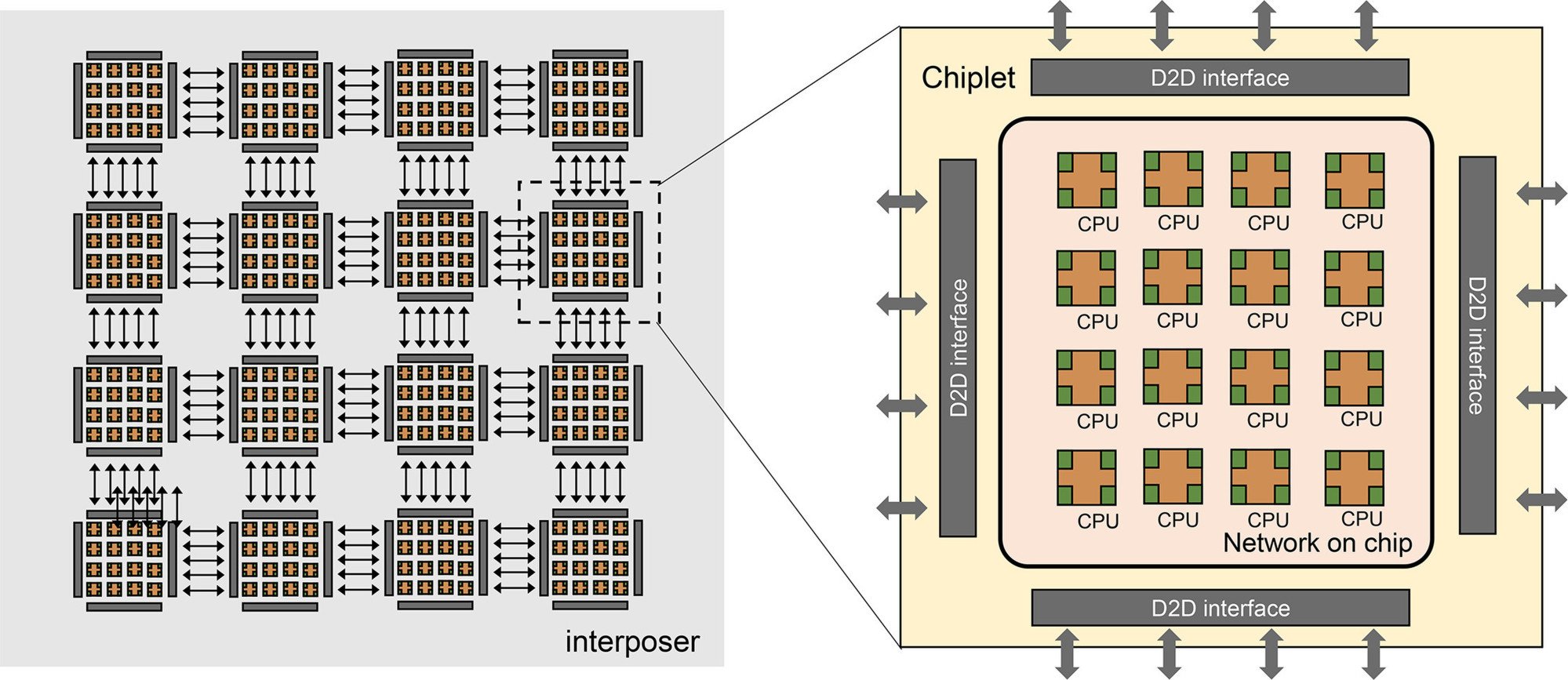
The Zhejiang covers an area measuring thousands of square millimetres and consists of 16 chiplets with 256 cores. The researchers also revealed it has the potential to scale up to 100 chiplets, corresponding to 1,600 cores in total.
“As Moore’s law comes to an end, the implementation of high-performance chips through transistor scaling has become increasingly challenging. To improve performance, increasing the chip area to integrate more transistors has become an essential approach,” wrote ICT professor Han Yinhe, the paper’s first author.
Moore’s law says the number of transistors in an integrated circuit doubles about every two years.
Big Chip refers to a chip that is bigger than the area limitation of the most advanced lithography machine available.
It has two main characteristics. First, the Big Chip is really big. Because of its size, it can have more tiny electronic parts, or transistors, than a regular single-piece chip made with existing technology.
Second, the Big Chip has multiple functional dies, and several emerging semiconductor fabrication techniques are used to integrate the prefabricated dies into a Big Chip.
Consisting of over a trillion transistors, the Big Chip can be created using two approaches.

“The second approach is wafer-scale integration (WSI), which involves building a very large integrated circuit from an entire silicon wafer,” Han said.
With WSI, the Zhejiang Big Chip processor is designed and fabricated on a 22nm CMOS process.
Because Big Chips contain more cores, the communication between cores will affect their cooperativity, so the architectural design of the chips has a significant impact on performance.
“It adopts a scalable tile-based architecture. The processor consists of 16 chiplets. In each chiplet, there are 16 CPU processors that are connected via a built-in network. And each tile is symmetrically interconnected with others to enable communication among multiple chiplets,” Han said in the paper.
“Moreover, this processor adopts a unified memory system, which means any core on any tile can directly access the memory across the entire processor.”
The chiplets are connected using a special system that lets them share communication paths one at a time. This method reduces the number of wires and connections needed, making the overall design simpler.
The paper gives an overview of Zhejiang’s architecture but the ICT website does not offer photos or an official release.
China’s semiconductor industry weathers tough year amid tighter US sanctions
Cerebras System, an American AI company, also uses WSI to build chips with an area up to 46,225 sq mm. They implemented Wafer-Scale Engine-1 (WSE-1) in 2019 and Wafer-Scale Engine-2 in 2021.
A complete system that contains WSE-1 was sold to the Pittsburgh Supercomputer Centre and US National Science Foundation in 2020 to build the AI supercomputer, Neocortex. The price tag was around several million dollars.
Big Chips are not without their challenges though.
While they can achieve a powerful computing ability, they still face yield, cooling and performance issues.
“Making big chips is complex and it’s hard to always do it perfectly due to many influencing factors. While there are ways to improve this, they can be costly,” Han said in the paper.
“Big Chips create a lot of heat, so it’s important to have good cooling systems and designs that use less power. Task mapping and design space exploration in Big Chip design are also challenging to implement.”


