Advertisement
Advertisement
Huawei
Get more with myNEWS
A personalised news feed of stories that matter to you
Learn more
Huawei Technologies Co’s semiconductor packaging innovation is expected to help alleviate its struggles with US chip sanctions. Photo: Shutterstock

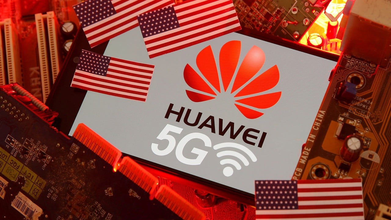
Chinese telecoms giant Huawei pushes semiconductor packaging innovation to ease disruptions caused by US chip sanctions

  • Huawei has filed a patent application on the mainland for ‘a type of chip stacking package and terminal device’
  • This innovation comes days after rotating chairman Guo Ping suggested that Huawei would use advanced chip packaging technology to help ease US restrictions
Huawei
Chinese telecommunications giant Huawei Technologies Co has filed a patent application on the mainland for a semiconductor packaging innovation, which industry analysts describe as a potential way to ease the disruptions caused by US chip sanctions on the firm’s operations.
The company’s patent application for “a type of chip stacking package and terminal device” is expected to help “solve the problem of high costs due to the use of through-chip via [also known as through-silicon via or TSV], while ensuring power supply requirements”, according to a statement released on Tuesday by the China National Intellectual Property Administration.
This innovation comes days after Huawei rotating chairman Guo Ping suggested at a press conference for the company’s annual report that it would use advanced chip packaging technology to help alleviate the firm’s struggles with US trade sanctions.
Privately-held Huawei, the world’s largest telecoms equipment maker and formerly China’s biggest smartphone vendor, was added to Washington’s trade blacklist in May 2019. The company has since scrambled to adapt its operations to tighter restrictions imposed in 2020, covering access to chips developed or produced using US technology, from anywhere.

05:22

Huawei founder on cybersecurity and maintaining key component supply chains under US sanctions

Huawei founder on cybersecurity and maintaining key component supply chains under US sanctions

Huawei did not immediately reply to a request for comment on Thursday.

TSV technology enables stacked chips to interconnect through direct contact, providing high-speed signal processing and improved photo detection for image sensing, according to a 2009 Institute of Electrical and Electronics Engineers paper. TSV was introduced into high-volume chip manufacturing during the past decade.

Huawei’s latest effort answers calls made by Chinese industry experts to pursue breakthroughs in chip assembly and packaging technologies at the World Semiconductor Conference, which was held in the eastern city of Nanjing in June last year. Advanced chip packaging, in which a set of integrated circuits are combined to form a powerful semiconductor, would help extend Moore’s Law, according to Jiangsu Changjiang Electronics chief executive Zheng Li, speaking on the sidelines of that event.
First observed by Intel co-founder Gordon Moore in 1965, Moore’s Law has become a “rule of thumb” on advances in computing power. It maintains that the number of transistors on a chip doubles roughly every two years, while the overall cost of that computing power halves.

“The main difficulty Huawei faces in terms of semiconductors is that advanced chips cannot be manufactured because of [current] equipment and foundry constraints,” said Wang Min, an expert in chip packaging technology.

Huawei CFO Meng Wanzhou says telecoms giant ‘more capable of dealing with uncertainty’

“One solution is to use larger nodes to produce chips at the expense of power consumption,” Wang said. “Another solution is to assemble different types of chips that can be bought in an SiP [System in Package] to make a complete final chip. This also sacrifices power consumption, but has advantages such as a shorter development cycle and lower final costs.”

Huawei’s consumer business, which includes smartphones, bore the brunt of US trade sanctions. This business saw its 2021 revenue plunge 50 per cent from a year earlier to 243.4 billion yuan (US$38.24 billion).

“We need to restructure our [tech] theories and architectures,” said Guo at the press conference last week. “We can trade ‘surface for performance’ and use ‘stacking’ for [improving] performance, to use less advanced processes and technologies to ensure Huawei products remain competitive.”

“This is the direction Huawei is heading,” said Guo, who shares the company’s rotating chairman title with Eric Xu Zhijun and Ken Hu Houkun.

Sanctions-hit Huawei loses ground in global telecoms equipment market

Huawei, meanwhile, is also strengthening its “legions”, an organisational model inspired by Google, to help boost revenue this year.

On Monday, Huawei announced the formation of 10 new legions, which puts its total number of specialist teams to 15. The new legions, which will focus on various digital transformation products and services, have a shorter reporting line to Huawei’s top brass, according to the company’s statement.

The new legions include teams on electric power digitalisation, one-stop public services, rail and aviation, interactive media, fitness and health, display chip, campus, wide area network and data centre bedrock.

1