Next-gen chip tech could be unlocked with 3D packaging tools from 80-year-old Japanese company
- Japanese toolmaker Disco is betting on 3D packaging for chips by stacking integrated circuits on silicon wafers of near-transparent thinness
- As Moore’s Law nears its physical limits, chip makers are looking at new materials and designs to get better performance out of next-generation hardware

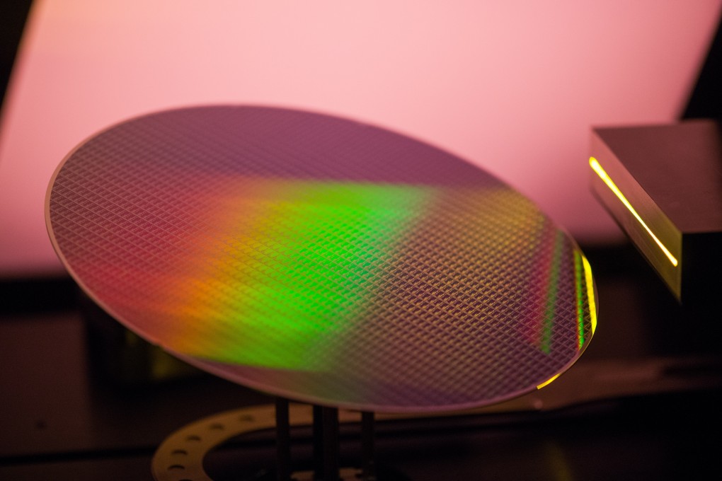
Disco Corp’s machines can grind a silicon wafer down to a near-transparent thinness and cut the tip of a hair into 35 sections. That know-how will allow chip makers to stack integrated circuits on top of each other in a process called 3D packaging, promising smaller chip footprints, reduced power consumption and higher bandwidth between various parts.
“Imagine having to cut a croissant cleanly in half,” Disco’s chief executive officer Kazuma Sekiya said in an interview. “That takes a special kind of knife and considerable craftsmanship.”
The semiconductor industry has long relied on Moore’s Law as a model for chip-technology breakthroughs, but makers are now approaching the physical limits of their ability to cram more transistors onto silicon as leaders like Taiwan Semiconductor Manufacturing Co migrate to ever-smaller nodes such as 3 nanometres. That’s prompting manufacturers to turn to solutions like 3D packaging to provide an edge. Disco’s technology has been in the making for four to five years and it’s finally ready for practical use, Sekiya said.
The small number of specialised machines Disco has already shipped have had very high gross margins, the CEO said, without providing details. Dicers are typically used toward the end of the fabrication process to cut individual chips from a wafer. Slicing more chips earlier in the process, where per-unit prices are higher, resulting in a boost for Disco’s revenues, he added, declining to give a specific timeline.

03:46
Taiwan’s worst drought in decades adds pressure to global chip shortage
“Disco has grown at twice the semiconductor industry’s pace because of this need for precision grinding and dicing equipment,” Damian Thong, an analyst at Macquarie Group Ltd, said. “Over the last 40 years, they have worked on every kind of cutting application imaginable, so they are well positioned for this next shift to 3D integration and packaging.”