Tech war: US, Taiwan, Japan gallop ahead in advanced semiconductors while China remains stuck at mature-node chips
- TSMC founder Morris Chang said this week that an expansion to the more advanced 3-nm process was planned for the company’s Arizona site
- China’s huge domestic market, especially lower-end segments served by legacy technology nodes, could provide a cushion for Chinese chip makers
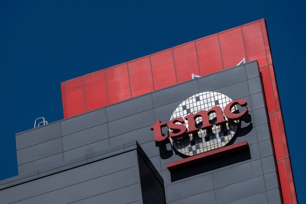
The chip technology gap between China and the West is likely to further widen as the US, Taiwan and Japan forge ahead with leading-edge projects while mainland Chinese foundries remain stuck at mature nodes due to US export controls, according to analysts.
At home, TSMC’s next-generation 3-nm process is expected to begin mass production in Tainan, southern Taiwan, in the second half of this year.
TSMC is developing the more sophisticated 2-nm process in Hsinchu, where its headquarters are located, while early stated 1-nm development is focused on a facility in Taoyuan, northern Taiwan.

Separately, eight Japanese heavyweights including Toyota Motor, Sony Group and telecoms giant NTT have formed a consortium to undertake 2-nm chip fabrication within the next five years, according to a report by Japanese public broadcaster NHK.
These forays by US allies into production of leading edge chips – used in high end smartphones and tablets – marks a sharp contrast to mainland Chinese wafer foundries that are being forced to stick with mature node chips due to US trade sanctions.
Analysts said the gap between China and global chip leaders is expected to widen further under the updated US restrictions that target advanced nodes, as foreign rivals will keep investing to push technology boundaries.
China’s top foundry, Semiconductor Manufacturing International Corp (SMIC), is only able to mass produce 14-nm chips – suitable for cars and home appliances – as it grapples with the challenges posed by the latest US sanctions.
China’s semiconductor industry on edge as US sanctions slow growth and demand
However, China’s huge domestic market, especially lower-end segments served by legacy technology nodes, could provide a cushion for Chinese chip makers.
“China’s response to the latest US sanctions in the chipmaking sector could be a retooling focus on mature nodes or third-generation semiconductors,” said Arisa Liu, a senior semiconductor research fellow at the Taiwan Institute of Economic Research.
Liu said that the Japanese chipmaking initiative, which is likely to source technology from US tech giant IBM, was “more symbolic” because of the high threshold to enter the advanced wafer foundry business, as well as the difficulties in aligning views from several companies.
The updated semiconductor export controls announced by the US Department of Commerce on October 7 sent a jolt through China’s chip industry, crushing its ambitions to achieve more self-sufficiency in a crucial sector that is at the heart of US-China tech rivalry.
TSMC has seen steadily increasing demand for its advanced capacity, defined as process nodes at 7-nm and below – which have become the workhorse for central processing units used in high-end smartphones and tablets.
TSMC’s combined revenue from 5-nm and 7-nm nodes accounted for 52 per cent of its total revenue in the third quarter.